 Tron Precision
CASE ANALYSIS
Case Study
Industrial CT Technology Leader
Site-wide search
CASE ANALYSIS
Industrial CT Technology Leader
Industrial CT inspection of IGBTs: Innovative application of high-precision non-destructive inspection technology
With the rapid development of modern manufacturing industry, the requirements for product quality and safety are becoming more and more stringent. In this context, industrial CT (Computed Tomography) technology has been widely used in many industrial fields with its advantages of high precision and non-destructive inspection.
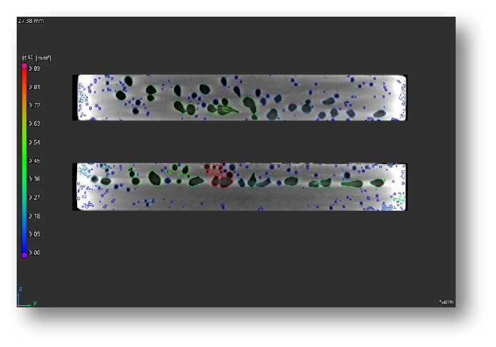
Industrial CT, the full name of industrial computed tomography, is a high-precision detection technology that utilizes radiation sources such as X-rays or γ-rays to penetrate an object and reconstructs the internal structure of the object through computer technology. Its basic principle is based on the attenuation and absorption characteristics of radiation in the detected object, through the detector received transmission energy, combined with computer information processing and image reconstruction technology, in the form of two-dimensional tomographic images or three-dimensional stereoscopic images, clear, accurate and intuitive display of the internal structure of the object to be detected, the composition of the material and the state of defects.
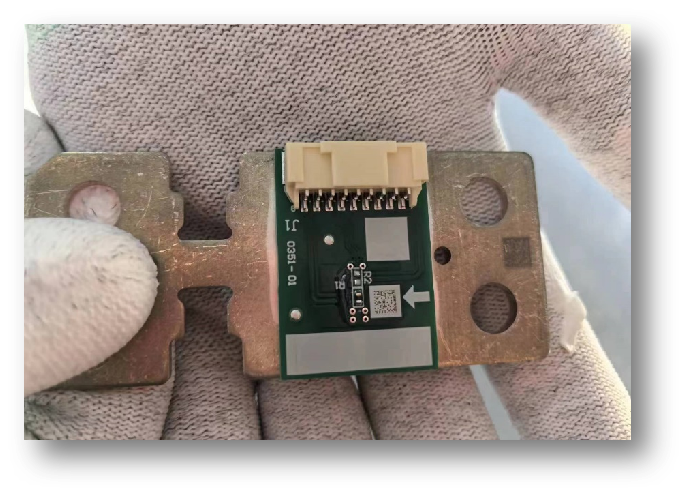
IGBT is a power semiconductor device, known as the "heart" of power electronic devices, widely used in high-speed rail, new energy vehicles, rail transportation, smart grid, aerospace and other fields. However, IGBT modules generate a lot of heat during operation, which needs to be dissipated in a timely manner, and the porosity of the solder layer will seriously affect the heat dissipation efficiency, which may lead to major safety accidents. Therefore, high-precision, non-destructive testing of IGBTs is particularly important.
Industrial CT testing of IGBTs offers the following significant advantages:
IGBT imaging after industrial CT scanning has several distinguishing features:

As the modern manufacturing industry's requirements for product quality and safety continue to improve, industrial CT, as an advanced nondestructive testing technology, will have broader application areas and market prospects. In the future, industrial CT technology will develop towards higher resolution, higher precision, faster imaging speed and more intelligent to meet the needs of different industries for inspection technology.
In the field of IGBT inspection, industrial CT technology will further improve the inspection accuracy and efficiency, reduce the inspection cost, and provide more reliable technical guarantee for the production and application of IGBT. At the same time, with the continuous progress of technology and cost reduction, the application scope of industrial CT inspection of IGBT will also continue to expand, contributing to the high-quality development of more fields.
In summary, industrial CT detection of IGBT is a technological innovation with broad application prospects and far-reaching significance. With the continuous development and improvement of technology, it is believed that this technology will play a more important role in the future and inject new vitality into the high-quality development of modern manufacturing industry.